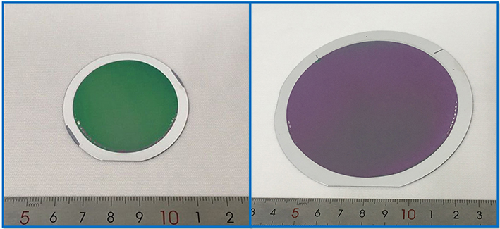
Fig. 1. In-situ fabrication of AAO templates on silicon wafers: (left) 2 inches, (right) 4 inches.
The preparation of AAO template by using high purity aluminium sheet has the advantages of good uniformity and good operability. However, the AAO template prepared from high purity aluminium sheet is difficult to be compatible with semiconductor technology, and it is not easy to obtain more precise and controllable micro-structures and micro-devices. Moreover, the ultra-thin AAO template prepared by aluminium sheet is easy to form wrinkles when transferred to the substrate, and the adsorption force is not strong, and the local area is weak. There may be disengagement. In order to remedy the above shortcomings, in-situ growth of AAO on substrates has been rapidly developed in recent years. The basic principle is to evaporate aluminium on the substrate and then prepare AAO, which is called AAO on substrate.

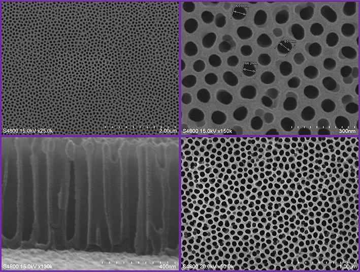
Figure 2. SEM diagram of AAO on Si substrate.
A silicon AAO product is introduced, as shown in Figure 1. There are two standard size silicon wafers, 2 inch and 4 inch. At present, the pore size can be adjusted from 30nm to 70nm (typical pore size is 30nm, 40nm, 60nm, 70nm), and the film thickness is about 500nm. As shown in Figure 2. Because the thickness of evaporated aluminium on silicon wafer can not be too thick, the pore arrangement and pore size uniformity of AAO prepared from thicker aluminium wafer are poor, but because of in-situ evaporation and growth, the bonding force between AAO and silicon wafer is very high, and the surface of AAO has no wrinkles and macro-fluctuations. At present, there is still a barrier layer at the bottom of the AO hole on the surface of silicon wafer. The through-hole product without barrier layer will be launched soon, please look forward to it.