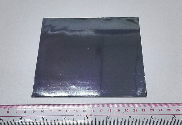
AAO on Al substrate has honeycomb-like structure (shown in Fig. 1), composed with hexagon column of Al2O3, with a circular pore in the center. At the end of the pore, there is a half-sphere shape barrier layer oxide layer in contact with aluminum. The porous oxide film contains mutually parallel cylindrical pores extending from the barrier oxide layer to the film surface. AAO on Al substrate is the simplest product in AAO family, which can be fabricated into large area with a high success rate. Fig. 2 shows a typical picture of the AAO template.

Fig. 1. Schematic of AAO on Al substrate.

Fig. 2. A large area AAO on Al substrate.
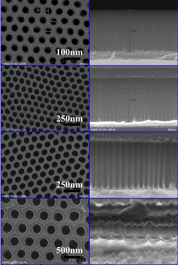
The pore diameter can range from 10 nm to several hundred nanometers, and the depth (or thickness of AAO) can be controlled continuously from several ten nanometers, up to one hundred microns. The pores of AAO on Al substrate is short-range ordered over a large area, which can be used as a master to transfer porous structures into other materials. The high density and high aspect ratio structure, provides a 3D nanostructure with a large surface-to-volume ratio, leading to high affinity of organic molecules. It has great potential in optical detection application. In addition, AAO on Al substrate can be used as a mask to electrically deposit nanowire with AC current.

Fig. 3. SEM images of some typical AAO on Al substrate.

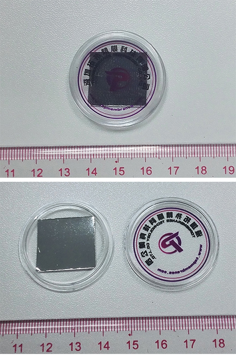
Fig. 4. A small area AAO on Al substrate.
AAO on Al substrate has highly ordered structure at one side (front side), with a barrier layer and aluminum as the support structure. The front side is facing to the logo in the package. Thanks to the support of aluminum substrate, it has a higher strength compared to other AAO products, which can be clamped by tweezers or cleaned with ultrasonic cleaner shortly. Again, don’t touch the surface with bare hand to avoid any dust or grease being introduced onto the surface.

Fig.5 The orientation of the AAO on Al substrate in the package.
AAO can be removed by 5% phosphate acid slowly, or by 5wt% NaOH quickly. You can image the structure with either SEM or AFM. Due to the non-conductive nature, the surface need to be sputtered with gold or carbon before SEM test. However, sputtering gold or carbon is not necessary if the thickness of AAO is less than 1μm.
The sample can be twisted into 90o to observe the cross section at the area cracked due to twisting. But this method is not suitable for AAO template whose pore wall thickness<20nm or='' pore='' depth=''>10μm.

Fig.6 The structure of a typical AAO on Al substrate