Using AAO as template, various one-dimensional nanomaterial arrays can be easily fabricated by electrochemical deposition. Generally, double-pass AAO templates are used. One layer of metal conductive layer is evaporated on the side of the template, and then nanomaterials are prepared by DC electrochemical deposition. However, double-pass AAO templates are fragile and inconvenient to operate. Evaporation of metal conductive layer also increases the cost and complexity of the experiment. If single-pass AAO templates can be used, the efficiency of the experiment will be greatly improved and the cost of preparation will reduce. However, in general, there is a thick barrier layer at the bottom of the single-pass AAO template hole. The layer of alumina insulation between the channel and the aluminium base is tens to hundreds of nanometers thick, which makes it difficult for electrons to pass through, even if AC electrochemical deposition is used, let alone DC electrochemical deposition.
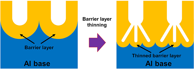
Figure 1. Schematic diagram of barrier layer thinning for aluminium-based single-pass AAO template
Because the thickness of the barrier layer of AAO template is related to the voltage used in the preparation, if the voltage is gradually reduced after the preparation of single-pass AAO template, the barrier layer can be thinned, thus obtaining "thin barrier layer single-pass AAO template", as shown in Figure 1. In recent years, this kind of single-pass AAO has been deeply studied and many reports have been published.
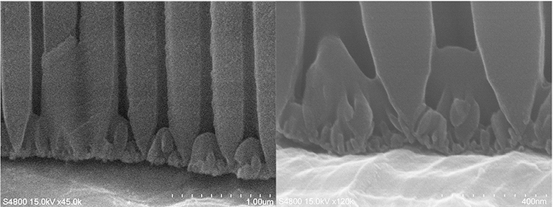
Figure 2. Typical SEM diagram of thin barrier layer single-pass AAO
We have successfully developed thin barrier layer single-pass AAO template through long-term experimental research. Fig. 2 is a typical high power SEM photograph of the bottom of thin barrier layer single-pass AAO template hole. At the bottom of the single-pass AAO channel, the fork becomes smaller, which is similar to the tree root. The closer the fork is, the higher the density of the hole is. The thinner the barrier layer is. The thickness of the barrier layer of our thin barrier layer single-pass AAO template is less than 10 nm. With such a thin barrier layer, the energy barrier is relatively low. In the electrochemical deposition process, electrons can easily pass through the barrier layer from the aluminium base.
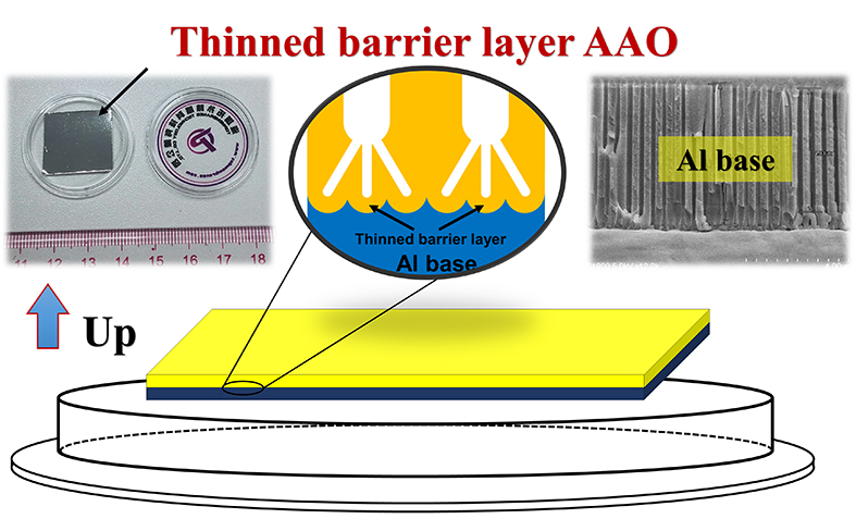
Figure 3. Diagram of the orientation of thin barrier layers in single-pass product packaging boxes
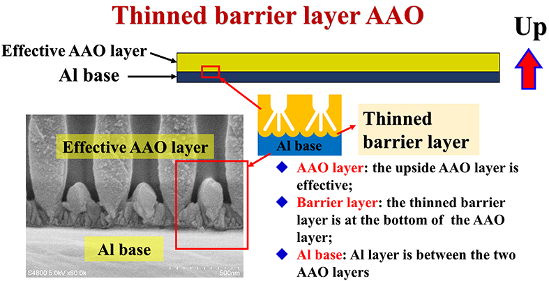
Figure 4. Overall structure sketch of single pass with thin barrier layer (effective AAO layer on the front and aluminium layer on the back)
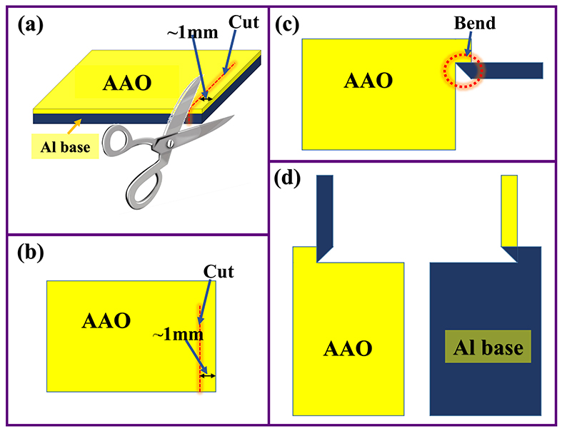
Fig 5. An example of a method for increasing the area ratio of thin barrier single-pass AAO samples immersed in electrodeposition solution. Yellow is AAO film and blue is aluminium base. (a, b) Cut a long strip on the side of the sample clean, (c) Flip and bend the small strip so that it is perpendicular to the side of the sample, (d) The positive and negative sketches of the sample after the side strip is turned. When the electrodeposition experimental circuit is connected, the negative electrode of the power supply is clamped on the top of the strip, and then the AAO sample is inserted into the electrodeposition solution. The electrode clamp does not touch the electrodeposition solution.
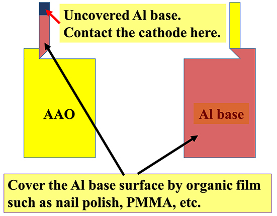
Figure 6. if the liquid on the back side of the sample is directly contacted on the back of the sample, the metal will be deposited on the surface of the backside aluminum substrate and affect the metal deposition in the positive AAO hole. Therefore, it is recommended to cover the back surface of aluminum base (including the edge side) with polymer insulation material, so long as the position of the top electrode clamp is not coated, the polymer material can be coated with nail polish or PMMA (solvents can be toluene, acetone, dichloromethane, chloroform, etc.) or glue, as long as it can play the role of isolation and sealing.

Figure 7. After the thin barrier layer deposits metal through a single pass, the morphology of the deposited metal nanomaterials has been observed by SEM of AAO cross section. The sample preparation method for measuring the cross-section of SEM is shown in the figure. The sample is cut into a rectangle by a vertical sample table. A 90°bend is formed on the vertical table. The AAO film will be broken at the bend, thus revealing a fresh cross-section. The conductivity must be increased by spraying gold after pasting the sample.
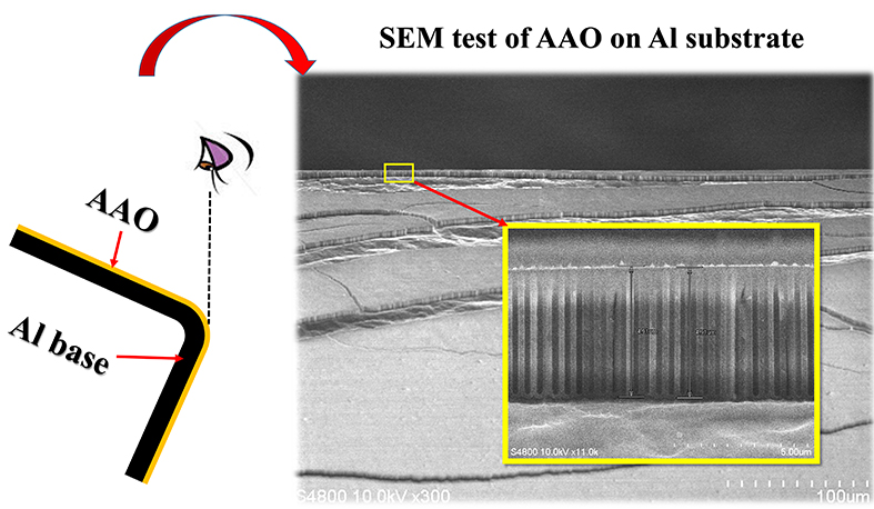
Figure 8. Practical operation method of SEM cross section measurement for thin barrier single pass products. When the sample is affixed to the vertical table, it is necessary to rotate the sample table 15-30 degrees along the horizontal axis in order to make the normal line of the bending section vertical upward so as to facilitate the observation of the selected area. Gold must be sprayed before SEM is used to measure the section to increase the conductivity. The common single-pass AAO is used in the figure. The thin barrier layer single-pass AAO test method is the same.
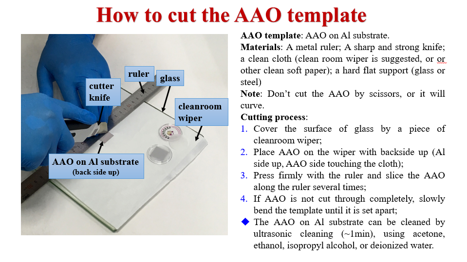
Figure 9. If the size of the sample required for the experiment is less than 20*20 mm, the sample needs to be cut down. Thin barrier layer single-pass cutting method is similar to ordinary single-pass AAO cutting method. Scissors should not be used. The back should be scratched with an artist's knife. When cutting, attention should be paid to keeping the sample clean and hands safe.
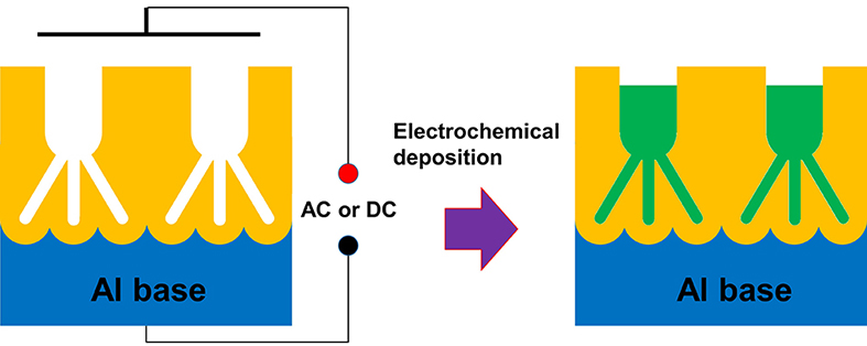
Figure 10. The schematic diagram of the preparation of nanomaterials by electrochemical deposition using thin barrier layer single-pass AAO as template
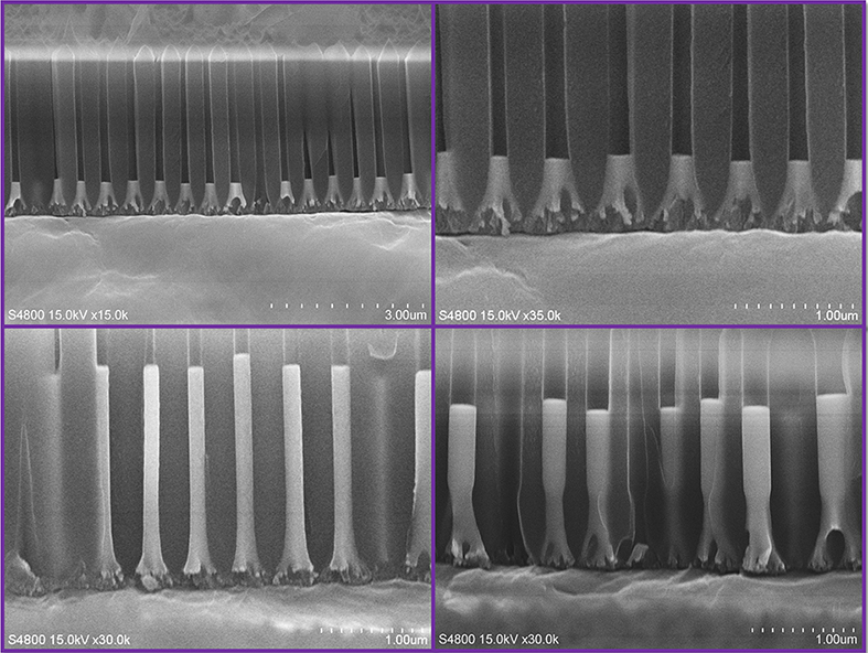
Fig 11. Nickel nanorods were prepared by direct current electrochemical deposition using thin barrier layer single-pass AAO as template. SEM image of AAO section was obtained after deposition.
The thin barrier layer single-pass AAO template is suitable for the preparation of nanomaterials by electrochemical deposition, and its principle is shown in Fig. 9. The AAO template is placed in the electrochemical deposition solution, and the template is connected with the power supply negative pole. By alternating current method (at this time there is no positive or negative pole) or direct current electrochemical deposition method, the electrons pass through the barrier layer to the electrochemical deposition solution, and the solution ions get electrons and precipitate. The target material can be obtained in the AAO channel. Due to the limitation of the AAO pore wall, a one-dimensional nanostructure array can be obtained.
Using nickel electrodeposition solution and direct current electrochemical deposition, nickel nanostructure arrays were obtained in thin single-pass AAO template holes, as shown in Fig. 10. Fig. 10 (a-c) template hole center spacing is 450 nm, hole diameter is 100 nm, Fig. 4D template hole center spacing is 450 nm, hole diameter is 200 nm. In the process of nickel deposition, the current density used is 8-30 mA/cm2 and the voltage is about 5-6.5V. Sometimes the current density can be 130 mA/cm2. There are several nano-thick alumina barrier layers at the bottom of the thin barrier layer, so the voltage of the thin barrier layer during electrochemical deposition is a little higher than that required for electrochemical deposition of double-pass AAO thick film with one side evaporated metal, please know. Here is just an example, and for nickel metal, the deposition conditions are not fully optimized. Customers can use AC or DC electrodeposition to optimize conditions and prepare nanomaterials such as Au, Ag, Cu, Pt, etc.
Reference:
Advanced Materials, 2000, 12, 582~586.
Nature Materials, 2009, 8, 648–653.
Journal of the American Chemical Society, 2010, 132, 13972–13974.
Nano Letters, 2017, 17, 523−530.
At present, the price is 140 yuan per piece, and the size is 20*20 mm square.
The spot models are as follows. Note: The marked hole depth here is about 5 microns. The actual hole depth fluctuates from 4 to 6 microns.
Type | Hole Center Spacing | Aperture Diameter | Hole Depth |
TBSP450-100-5000 | 450nm | 100nm | 5000nm |
TBSP450-200-5000 | 450nm | 200nm | 5000nm |
TBSP450-300-5000 | 450nm | 300nm | 5000nm |
TBSP450-400-5000 | 450nm | 400nm | 5000nm |