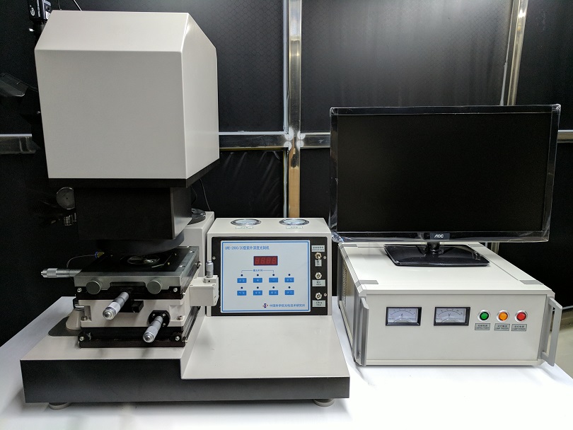
At present, our company has completed the construction of our clean room, and can provide various micro-machining services and customize products for customers, including:
Photolithography: Ultraviolet photoresist is used to develop and form the same or complementary structures as those on the mask. With a high-precision photolithography machine, the current fabrication accuracy is less than 2 μm, the area size varies from small area to standard 4-inch, the design and ordering of lithography mask are provided as well.
In addition, we sell a series of photolithography machines, which can be configured according to your research funding and specific needs. For more details, please contact us.
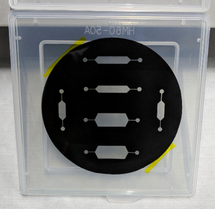
Lithography mask
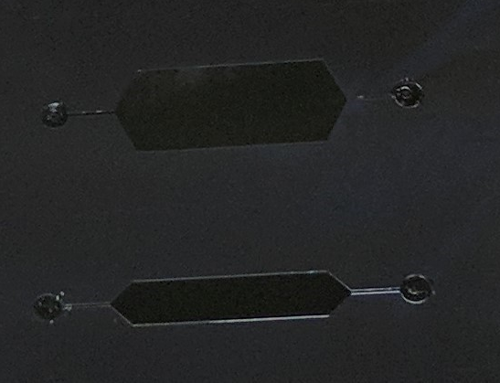
Lithographic microstructure
Soft lithography: Based on photolithography and PDMS inversion process, according to the specific design of users, microfluidic chips or other devices are fabricated on the base (silicon wafer, glass) to achieve rapid prototyping. Unique inlet/outlet integration technique enables easy and reliable input/output without leakage.
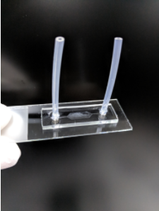
Microfluidic chip
Microfluidic chips: Using precise CNC technology, microfluidic chips can be machined including standard chips, chemical reaction chips, analysis and detection chips, drop forming chips, cell analysis chips, concentration gradient chips, electrophoresis chips, etc.
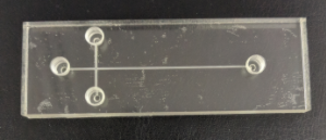
Cross chip
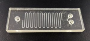
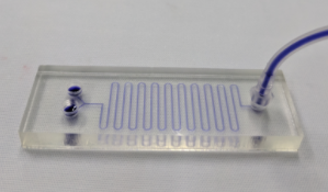
S chip
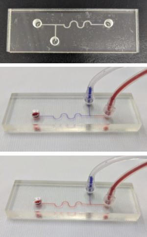
T chip
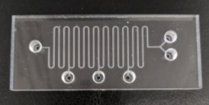
Multi-Inlet Hybrid Chip
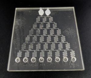
Concentration gradient chip
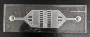
Cell analysis chip
Spin coating: an important step in the manufacture of MEMS. Spin coating plays a critical role in photolithography and the quality of final products. Our company provides professional spin coating with high uniformity and adhesion, covering sample size from 1 cm to 4-inch.
Direct Laser Writing: Masks used in photolithography are usually provided by special suppliers. In the R&D environment, the design of masks often needs to be customized. Direct laser writing technology overcomes this problem by designing structure pattern with software. Unlike exposure through a physical mask, direct laser writing directly write the designed patterns on the photoresist using compute-controlled laser pulses.
Electron beam evaporation: Electron beam evaporation is a kind of physical vapor deposition (PVD), which uses accelerated electron to bombard coating materials. Using electromagnetic field, high energy electron beam can be accurately focused on the target in the crucible, which can evaporate into gaseous state and deposit on the substrate. Electron beam evaporation can deposit thin films with high purity and precision. Compared with thermal evaporation, the electron beam only heats a small part of target material and thus releases relatively less energy. Accurate aiming of the electron beam on the target can also avoid introducing pollution into the crucible.
Nano-imprinting: Transfer the pattern to the substrate covered with the resist under certain pressure through a prefabricated imprint template. Imprinting is usually on a thin polymer film, which is hardened by hot embossing or ultraviolet irradiation to retain the transferred pattern. The entire process includes three main steps: stamping, demoulding and etching. Nanoimprinting has solved the difficulties of traditional photolithography when the feature size further reduces to the nanometer range, and has advantages of high resolution, low cost and high yield.